Ion Beam Figuring: New Applications and Developments for Quantum Technologies


Modern optical systems are facing rapidly growing demands — especially in fields such as aerospace, quantum technologies, and laser applications. These demands increasingly require highly complex freeform optics with extreme form accuracy and surface quality. Traditional manufacturing technologies are reaching their limits when it comes to processing these advanced components, often involving overall long processing times and limited flexibility for highly precise shaping.
The talk “From Precision to Power: Ion Beams in Extreme Material Removal Applications” introduces a cutting-edge approach that addresses these challenges: the use of focused ion beams for precise (a)spherization and shaping of optical surfaces, even under conditions requiring high material removal rates.
At the core of this innovation is the further development of Ion Beam Figuring (IBF) – generally used for nanometer-scale surface correction. By implementing advanced ion extraction systems with significantly increased ion current densities, material can now be removed with high precision and efficiency. This enables a controlled, localized shaping process, drastically reducing overall machining time while maintaining optical quality. Additionally, further optimization and finishing is possible using the same machine; just the need of changing the ion beam source configuration.
The presentation highlights how this method is effective not only for small precision optics, but also for larger-scale components with aspheric geometries. Real-world examples from current research and development projects illustrate the actual state and benefits of this approach.
Finally, the talk outlines the potential for industrial scaling, addressing how the balance of precision and throughput opens up entirely new possibilities for future optical fabrication in demanding high-tech sectors.
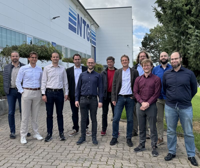
We just wrapped up the second project meeting at NTG, and the team is making great progress!
Our mission: build an industrial optical toolbox using thin-film lithium niobate (LNOI) to create fast, scalable, and flexible photonic circuits for HPC, AI, quantum tech, and beyond.
This disruptive, non-CMOS platform paves the way for resilient, local production of photonic chips in Germany and the EU.
We’re proud to collaborate with Institut für Mikroelektronik Stuttgart (IMS CHIPS), Universität Stuttgart, Q.ANT GmbH, Friedrich-Schiller-Universität Jena and Menlo Systems – a true cross-regional effort across Baden-Württemberg, Hessen, Thüringen, and Bayern. Funded and supported by Bundesministerium für Forschung, Technologie und Raumfahrt (BMFTR).
The LichtBriQ team is turning innovation into reality — stay tuned!

You need to load content from reCAPTCHA to submit the form. Please note that doing so will share data with third-party providers.
More InformationYou are currently viewing a placeholder content from Turnstile. To access the actual content, click the button below. Please note that doing so will share data with third-party providers.
More InformationYou are currently viewing a placeholder content from Facebook. To access the actual content, click the button below. Please note that doing so will share data with third-party providers.
More InformationYou are currently viewing a placeholder content from Instagram. To access the actual content, click the button below. Please note that doing so will share data with third-party providers.
More InformationYou are currently viewing a placeholder content from X. To access the actual content, click the button below. Please note that doing so will share data with third-party providers.
More InformationYou need to load content from reCAPTCHA to submit the form. Please note that doing so will share data with third-party providers.
More Information